Transistors are at the very core of today's electronics technology. The development of the transistor has resulted in many changes to the world.
The introduction of the transistor has enabled many technologies we take for granted today: everything from portable transistor radios, through to cellular phones, and computers, remote operation, the functionality we take for granted in current day automobiles, etc . . . . All these and many more everyday items have all been made possible by the invention of the transistor.
Plastic leaded transistor selection
Today, transistor are available in many forms. There is the basic transistor in a leaded form or as a surface mount transistor. But transistors are also widely used within integrated circuits. Most digital ICs use field effect technology, but many analogue ICs use bipolar technology to provide the required performance.
Transistor development
Semiconductor technology is now well established but it has been used for over a hundred years. The first semiconductor effects were noticed back in the early 1900s when the first wireless or radio sets were being used. Various ideas were being investigated as detectors. Thermionic valve or vacuum tube technology was introduced in 1904, but these devices were expensive, and also required powering by a battery. Soon afterwards the Cat's Whisker detector was discovered. This consisted of a thin wire placed onto one of a number of types of material. These materials are known today as semiconductors and form the basis of modern electronics technology.
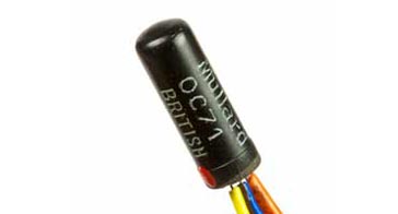
Old OC71 transistor
After the basic idea was developed, it took some time before semiconductor technology was adopted, but once it was, it took off in a major way as we know today.
What is a bipolar transistor
A bipolar transistor needs to be differentiated from a field effect transistor. A bipolar transistor gains its name from the fact that it uses both holes and electrons in its operation. Field effect transistors are unipolar devices using one or either type of charge carrier.
A bipolar transistor, or more exactly a bipolar junction transistor, BJT, has two diode junctions which are back to back. The bipolar transistor has three terminals, named the emitter, base and collector.
The transistor amplifies current - bipolar transistors are current devices, unlike thermionic valves vacuum tubes, and FETs which are voltage devices. The current flowing in the base circuit affects the current flowing between the collector and the emitter.
Basic transistor structure
The transistor is a three terminal device and consists of three distinct layers. Two of them are doped to give one type of semiconductor and the there is the opposite type, i.e. two may be n-type and one p-type, or two may be p-type and one may be n-type.. They are arranged so that the two similar layers of the transistor sandwich the layer of the opposite type. As a result transistor are designated either P-N-P (PNP) types of N-P-N (NPN) types according to the way they are made up.
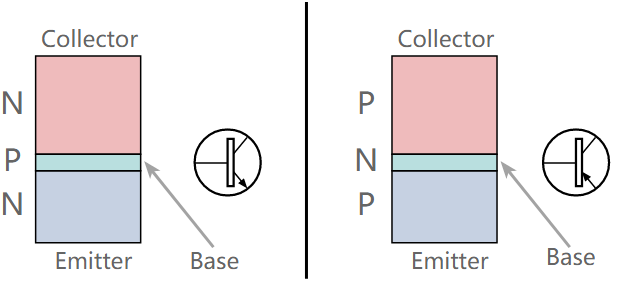
Transistor basic structure and circuit symbols
The names for the three electrodes widely used but their meanings are not always understood:
-
- Base: The base of the transistor gains its name from the fact that in early transistors, this electrode formed the base for the whole device. The earliest point contact transistors had two point contacts placed onto the base material. This base material formed the base connection . . . and the name stuck.
- Emitter: The emitter gains its name from the fact that it emits the charge carriers.
- Collector: The collector gains its name from the fact that it collects the charge carriers.
For the operation of the transistor, it is essential that the base region is very thin. In today's transistors the base may typically be only about 1µm across. It is the fact that the base region of the transistor is thin that is the key to the operation of the device
Transistor basics: operation
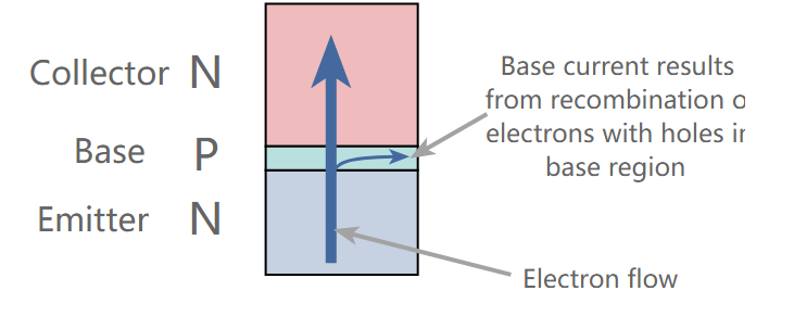
A transistor can be considered as two P-N junctions placed back to back. One of these, namely the base emitter junction is forward biased, whilst the other, the base collector junction is reverse biased. It is found that when a current is made to flow in the base emitter junction a larger current flows in the collector circuit even though the base collector junction is reverse biased.
For clarity the example of an NPN transistor is taken. The same reasoning can be used for a PNP device, except that holes are the majority carriers instead of electrons.
When current flows through the base emitter junction, electrons leave the emitter and flow into the base. However the doping in this region is kept low and there are comparatively few holes available for recombination. As a result most of the electrons are able to flow right through the base region and on into the collector region, attracted by the positive potential.
Basic transistor operation
Operation shown for NPN transistor
Only a small proportion of the electrons from the emitter combine with holes in the base region giving rise to a current in the base-emitter circuit. This means that the collector current is much higher.
The ratio between the collector current and the base current is given the Greek symbol Β. For most small signal transistors this may be in the region 50 to 500. In some cases it can be even higher. This means that the collector current is typically between 50 and 500 times that flowing in the base. For a high power transistor the value of Β is somewhat less: 20 is a fairly typical value.