Our hands have all experienced electrostatic discharge (ESD). Even just walking over a carpet and then touching certain metal parts will release the accumulated static electricity in an instant. Many of us have complained about using conductive blankets, ESD electrostatic wristbands, and other requirements in the lab to meet industrial ESD standards. Many of us have also damaged expensive electronic components due to careless use of unprotected circuits.
ESD is a challenge for some people because it needs to be handled and assembled without causing any damage. This is a circuit design challenge because it is necessary to ensure that the system can withstand the impact of ESD and then still work normally. It is better that no user-detectable faults occur after an ESD event.
Contrary to common sense, designers can completely prevent the system from malfunctioning and continue to operate after an ESD event. With this goal in mind, let's better understand what exactly happened when the ESD hit, and then introduce how to design the correct system architecture to deal with ESD.
▼ Simple model
Charge a capacitor to a high voltage (typically 2kV to 8kV), and then close the switch to release the charge into a "damaged" device that is ready to withstand ESD shocks (Figure 1). The polarity of the charge can be positive or negative, so you must handle both positive and negative ESD situations.
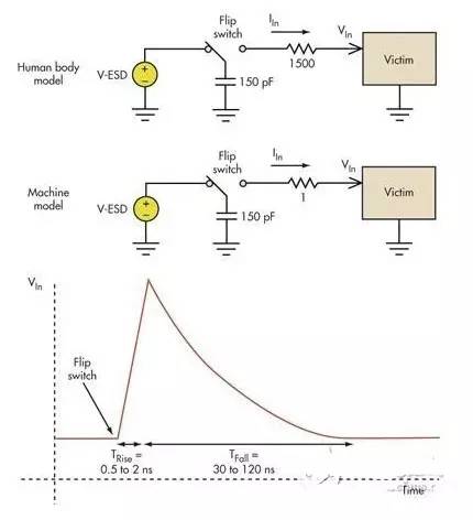
Figure 1: Board-level ESD typically involves machine models (MM) and human models (HBM).
The high transient voltage that destroys the damaged circuit generally has a rise time of several nanoseconds and a discharge time of about 100 nanoseconds. Unlike damaged circuits, the sensitivity to positive and negative shocks may also be very different, so you need to deal with Good positive and negative impact. The difference between the two most common models, the Human Body Model (HMB) and the Machine Model (MM), is mainly in series resistance. Human models are not as conductive as metals.
The best protection against overvoltage damage is voltage limiting or clamping with a non-linear circuit (Figure 2). The most commonly used are specialized diodes that have very low impedance when forward biased or in the Zener breakdown region. The introduction of a voltage limiter can cause some other events quickly, because large surge currents through the capacitor discharge through the voltage limiter.
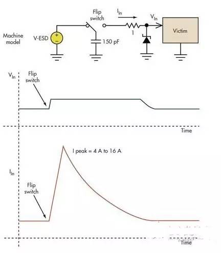
Figure 2: Basic voltage limiting circuit prevents overvoltage damage
Although high transient voltages are eliminated, replacing them with a few amps of inrush current may cause other problems in the system. Depending on the total impedance of the subsequent path, the inrush current can reach several amps. When designing an I / O unit for a chip, you often see 4A to 16A inrush current into the device. Dealing with such huge transient inrush current has become a big problem in ESD design. Limiting the voltage is relatively easy, but the resulting current may reverse the circuit and ground elsewhere in the system.
The current forced into the ground by the voltage limiter will cause inductive ringing in that node of the system (Figure 3). The power supply typically travels along the ground and is a function of the power supply's decoupling capacitors, so the core of the system still works. However, the control lines connected to the board may be confusing because they are established relative to the ground off-board. As a result, an ESD event may occur at a location and cause an input terminal on the board to appear to malfunction.
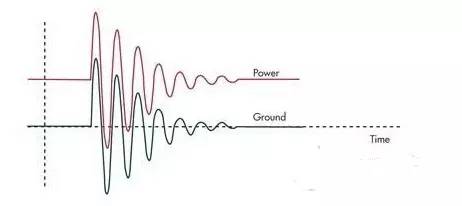
Figure 3: Injecting a large inrush current into the ground through a voltage limiter will cause the PCB ground to bounce and appear as a function of the connected inductor
▼ The role of the fort
With board-level ESD, you can try to build a fort and set up multiple controlled access points on the "moat". The parts connected outside the "city wall" can be broadly divided into several categories: protocol-controlled data, low-bandwidth detection and control lines, and high-speed interfaces. The first two are relatively easy to deal with, and the third is somewhat challenging. There are several different ways to protect these three parts from ESD damage.
Regardless of the end product, some form of protective enclosure will be part of the device. Isolating the circuit inside the enclosure is the first line of defense that needs careful consideration. In the ideal case, the metal shell connected to the circuit board can usually be used, but modern products often use non-conductive plastic or other modern materials.
Circuit designers often have no control over the materials used to build the walls, but they have an inescapable responsibility for protecting the fort. When designing the case, you need to pay attention to the ESD that reaches any part of the outside of the case, there are countless paths into the internal circuit.
Building a fortress where the PCB can protect itself from ESD strikes can begin with a low-impedance grounding method. Establishing a ground and normal power integrity allows the printed circuit board (PCB) to maintain signal integrity throughout the board, even when subjected to large ground surge currents.
As a design engineer, you will ask everyone to fasten their seat belts so that they can handle a small amount of airflow. The plane may sway up and down quickly, but if everyone fastens their seat belts, everyone will stay in place and the plane will continue to fly. After that, you need to protect external connections and limit the effects of ESD events.
The protection circuit should be located at the board entry point, not downstream of the entry point. What needs to be dealt with is the potential of several thousand volts caused by arcing problems, or the surge current of several amperes which is best handled at the edge of the board.
▼ TVS voltage limiter
A transient voltage suppression (TVS) limiting diode can be used as a voltage limiter. They are divided into normal voltage, logic level and power supply voltage. Common voltage types are: 12V, 5V, 3.3V, 2.5V, 1.8V, and 1.2V.
This number should look familiar because these devices are specifically designed for the needs associated with many CMOS devices. One specification cannot meet all requirements, they should be the correct voltages to protect the device.
The modern CMOS process significantly reduces the power supply voltage to protect transistors without many design margins and limited voltage range, which is worthy of our respect. These devices are typically manufactured using foundry processes that can provide high-current devices with low impedance characteristics in small packages.
Placing a TVS voltage limiter on the input line protects the input from damaging ESD damage (Figure 4). But this kind of voltage limiter can not deal with the signal chaos that occurs when the host is processing, nor can it deal with the reverse effect caused by the huge ground current surge.
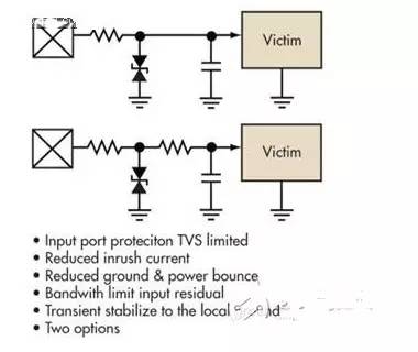
Figure 4: A simple voltage-limiting voltage can provide over-voltage protection, but may cause inrush current problems. Inrush current should be limited and the signal should remain relatively local ground stable
As mentioned earlier, the performance difference between HBM and MM is very large. In many cases, adding some series resistance before the TVS device will help limit current surges and reduce ground bounce. As with HBM, the end result is reduced system stress.
Often bandwidth limitations by themselves will not solve the ESD problem. Low-pass filter attenuation of small ESD also requires 60dB to 150dB to eliminate transient voltage, which is difficult for simple passive filters. The TVS voltage limiter can pull the signal between the power rails.
First-order RC circuits can then be used to maintain signal integrity (Figure 4). The capacitor can also stabilize the input voltage with respect to local ground. This method provides good protection for a large number of low-bandwidth inputs, including "set and forget" control lines, sensor inputs, and similar objects.
Although most of what we discuss is protecting the input ports of the PCB, the output port protection is similar. TVS voltage limiters and additional resistors are also suitable here. Limiting the voltage helps prevent semiconductor damage and protects other components with voltage limits.
Series resistance also helps stabilize the ground. In addition, keeping the ESD surge current away from the I / O unit of the digital chip can prevent the ground wire from bounced inside the chip, allowing the processor to maintain normal operation when the external voltage limiter absorbs the surge current surge.
▼ ESD inside the chip
The ESD protection function inside the IC is somewhat compromised for a number of reasons. Both silicon and metal are optimized for the core functions of the IC and are not suitable for high current operation. Special TVS devices use silicon optimized for high-current circuits and have higher performance than PN junctions in ordinary CMOS.
In addition, an I / O unit with a large current ESD protection function will occupy a considerable amount of space, thereby driving up the cost of the IC. And high-frequency pins on ICs usually cannot add large-sized ESD protection circuits because it will generate capacitive loads.
As a general experience, the degree of ESD protection inside the chip is just enough to complete the IC production and solder to the PCB, but it lacks the robust protection performance usually required by the application environment. If the connection needs to leave the PCB, external devices are usually required for further protection.
▼ Data communication port
A properly designed communication port will use a robust protocol, which includes a common use of cyclic redundancy check (CRC) encoding to test the integrity of the data. The Ethernet, USB and CAN buses have been developed with CRC encoding and transmitted with the data. A properly designed receiver will check if the CRC encoding matches the data sent. If they do not match, it means that either the data or the CRC encoding has an error and a request to resend the data will be issued.
Because ESD events last less than 100ns, the CRC check, verification, and retransmission processes typically process ESD in an invisible manner. End users are generally unaware that the corrupted information has been corrected. There are no protective measures in the structure of other protocols.
I2C, Serial Peripheral Interface (SPI), and System Management Bus (SMBus) communication designs work on the PCB and cannot verify and correct data. If some data is leaving the board, make sure you have a way to verify the validity of the data.
Most modern communication paths use a differential approach, which uses some form of low-voltage differential signaling (LVDS). Each LVDS connection needs to be protected by TVS like all other signals. Magnetic field isolation (common to Ethernet) and common-mode chokes help resolve common-mode changes due to ground bounce in ESD events. When the input signal and the PCB do not share the same ground, optical or magnetic isolation measures should be taken.
High-speed data streams that require perfect data integrity but do not include error checking are particularly difficult to prevent ESD shocks. Understanding how the device provides serial data rates greater than 1GB / s and complete communication protocol protection can avoid this problem.
▼ Analog Signal and Digital Intelligence
Any analog signal leaving or entering the board needs basic TVS protection. The bandwidth of the connected channels needs to be considered to determine what other steps should be taken next. Most analog control signals, motion control systems, audio, and indicators do not require additional measures because the response time of the device used is longer. The RF front end is the physical layer of the communication channel, and self-correction is provided by an error detection mechanism as part of the protocol.
Hardware can only provide so much protection. If a processor in the system center needs to complete monitoring and control, then some options are needed. The techniques described here can make your processor no longer lost or need to go through a reset cycle. What happened under the control of this host is another thing to consider.
In general, you need to program some intelligence into the processor code so that it can identify the wrong information and handle it correctly. The time-division polling port can easily solve the problem of slow detection and control lines. Because the ESD event is very short, if the data on the port remains stable for multiple samples within a few milliseconds, then the system will not have such a catastrophic event.
In addition, the output can be refreshed as part of the reproduction process. This step is not needed if the processor is a memory unit, but if the data is locked remotely, a refresh routine is needed to manage the destruction event